Semiconductor Metrology Systems
PROFORMA SERIES
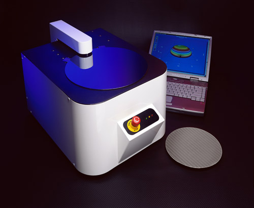
The Proforma 300SA is a semi-automated thickness measurement system for both semiconducting and semi-insulating wafer materials. Capable of handling 200 mm and 300mm wafers, the 300SA provides highly accurate, repeatable measurements of thickness, TTV, bow, warp, site and global flatness. Built around MTI Instruments' exclusive Push-Pull capacitance technology, the Proforma 300SA delivers full wafer surface scanning at the press of a button. User defined and ASTM/SEMI scan patterns are used to generate a full 3-dimensional image of the wafer.
Easy to Use....
The standard Windows® user interface makes the Proforma 300SA easy to use and set-up. Each measurement and machine parameter is selectable from a list of standard options. The control software has three levels of security, from a production environment to a full engineering analysis of wafer geometry. Customized data reports, as well as the ability to export measurement data to any spreadsheet add the ability to match the Proforma 300SA to your process needs
Wafer Specifications
- Diameter: 200mm and 300mm.
- Material: All Semiconducting and Semi-insulating materials.
- Surfaces: As-cut, Lapped, Etched, Polished, Patterned.
- Flat/Notch: All SEMI Standard Flat(s) or Notch.
- Conductivity: P or N Type.
- Wafer mounting: Bare Wafer, Sapphire/Quartz Base, Tape.
Measurements
- Thickness and TTV.
- Bow
- Warp
- Site and Global Flatness
Advantages
- Cost effective alternative to fully automated tools.
- Full 1000 uM Thickness Measurement Range without re-calibration. Extended range models available for thickness range to 1.7 mm.
- Standard Windows® User Interface.
|