ºñÁî´Ï½º 778

ACO

AMETEK

APPLIED MEMBRANES

AMITTARI

ARCOTEST

BALMAC INC

BECKMAN COULTER

BJORNAX AB

BW TECHNOLOGIES

CHEM INSTRUMENT

DAKOTA ULTRASONICS

DCS INC

DEFELSKO

DIAVITE AG

NIPPON DENSHOKU

ECOPIA

EGG TESTER

ELCONTROL ENERGY

EIT INC

ETS-LINDGREN

FOURIER SYSTEM LTD

FOURTEC

GALLTEC + MELA

GE SENSING

GRANT INSTRUMENTS

HYDRONIX

IET (IDENSHI)

IKM INSTRUTEK

IMV CORPORATION

INSTRUTECH INC

ION SCIENCE

JFE ADVANTECH

KELLER

LIST-MAGNETIK

METONE

MICRONICS LTD

MIKRON

MTI INSTRUMENT INC

NITTOSEIKO ANALYTECH

OKANO WORKS

ONO SOKKI

PCWI

PINION PRODUCTS CORP

RALSTON INSTRUMENTS

RM YOUNG

SCANSENSE

SHAW MOISTURE METER

SHOTOX

SHOWASOKKI CO LTD

SHINYEI KAISNA

STRESSTEL

TESTO

TRAFAG

TREK INC

UE SYSTEM

ULVAC

WILDCO

ZAWADA NDT

OTHER MAKER

 
Semiconductor Metrology Systems ¢¹ Semiconductor Metrology Systems
Semiconductor Metrology Systems
  ¸ðµ¨¸í : PV-1000
  ¿ø»êÁö : ¹Ì±¹
  Á¦Á¶»ç : MTI INSTRUMENT INC
  °¡   °Ý : ¹®ÀÇ(031-753-9550)
  ºÐ·ù¸í : Semiconductor Metrology Systems
product
Á¦Ç°»ç¾ç
Àû¿ë»ç·Ê
±â¼úÀÚ·á


Semiconductor Metrology Systems

Proforma 300

The PV-1000 Advantage

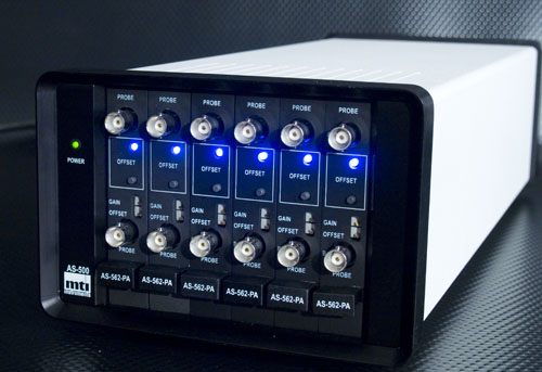
Using MTII's exclusive Push/Pull capacitance probe technology, each PV-1000 module provides up to three pairs of probes for measurement of maximum, minimum and average thickness, as well as total thickness variation (TTV) and wafer bow. For applications requiring additional thickness channels, multiple PV-1000 modules can be chained together for unlimited line scans on the wafer.

Wafer saw mark detection and classification is accomplished by adding optional laser sensors to the PV-1000 module. Utilizing up to two of MTII's industry leading Microtrak – SA standalone laser heads, saw marks can be classified for orientation and depth simultaneously with wafer thickness scanning making the PV-1000 ideal for incoming wafer characterization and sorting.

Integrated data acquisition and control electronics analyze and transmit wafer data via the on-board Ethernet port at speeds of up to five wafers per second. The digital I/O port allows communication with wafer handling equipment for up to 64 classes of wafer sorting and binning. Remote monitoring capabilities allow you to see your production line data across your network or directly at the module.


  • Up to three thickness channels per rack
  • Exclusive MTII push/pull capacitance probes work with all wafer types
  • Minimum, maximum, average and total thickness variation measurements
  • Bow measurement (3 probe pairs required)
  • Optional laser sensors for wire saw orientation and depth monitoring
  • Integrated data aquisition and control electronics
  • Fast Ethernet communications ports for production rates up to 5 wafers per second
  • Scalable for increased number of thickness line scans
  • Digital I/O for interface with existing wafer handling equipment
  • Windows¢ç based control program for local or remote data monitoring
  • Windows¢ç based DLL package for integration with existing control PC's
  • Standard and custom probe sizes available


  • Slicing
    • Saw set-up
      • Thickness
      • TTV
    • Degradation monitoring
      • Wire guide re-grooving
      • Blade replacement
  • Lap/etch and polishing
    • Process monitoring
    • Thickness
    • TTV
    • Removal Rate
  • Final Inspection
    • Lot sampling
    • Final thickness